
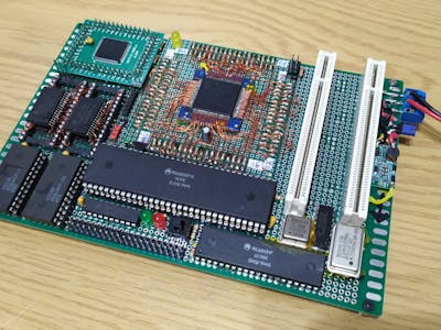
Bus protocols are where a lot of ECE students hit a wall. You can read the PCI specification for a week and still have no picture of what happens on the actual wires. Piotr Grzesik’s answer was to build one: a hand-wired Motorola 68000 computer with two working PCI slots, pairing a 1979 CPU with a bus that showed up more than a decade later. PCI was designed to be processor-independent, so nothing in the spec forbids it.
What he actually built
The whole machine sits on a 12 x 18 cm prototype board, assembled by hand from parts already in the bin. A 10 MHz 68000 runs the show, backed by 1 MB of SRAM, 4 KB of ROM, and an MC68681P DUART covering serial, timing, and I/O. Before any of that, Grzesik reverse engineered a proprietary PCI card built around a Xilinx Spartan II XC2S100 FPGA and wrote his own VHDL implementation of the protocol, pushing until a PC recognised the card, handed it a Base Address Register, and read its internal memory.
Two buses that disagree
An XC95144XL CPLD handles glue logic and interrupt routing. A Spartan II XC2S100 acts as the PCI host bridge, turning 68000 bus cycles into PCI configuration, I/O, and memory transactions. The two 32-bit 5V slots run at 10 MHz rather than the standard 33 MHz, which keeps the PCI clock locked to the CPU and removes a pile of FPGA logic. The nastier problem is endianness. The 68000 is big-endian and PCI is little-endian, so the bridge applies different byte-ordering schemes depending on the access type. There is no bus mastering and no DMA, but interrupts work: each slot gets its own CPU interrupt level, with that slot’s four INTx lines tied together.
Those limits still leave room for real hardware. A MosChip NM9835 serial card runs fine, so do Cirrus Logic GD5440 and S3 Trio64V2/DX graphics cards, and an obscure IGS IGA 1680_A was coaxed into 80×25 colour text. An RTL8029 Ethernet card puts the 68000 on a network with a Telnet console and an HTTP server, precisely because NE2000-compatible controllers skip DMA.
Build a smaller version of this
Start with a 68000 single-board computer on perfboard: CPU, SRAM, ROM, and a DUART for a serial console is a complete weekend build and already teaches address decoding. Add a cheap XC9500XL or MachXO2 CPLD board for chip-select and interrupt glue rather than a stack of 74-series logic. Keep a logic analyser on the address strobe lines, because a wrong decode window looks identical to dead RAM. Once serial output works, an ISA or PCI bridge becomes a firmware problem instead of a wiring problem. The full source, including the FPGA and CPLD logic, bootloader, PCI subsystem, and drivers, is open on GitHub, linked from the writeup at Hackster.
Frequently Asked Questions
Why do the PCI slots run at 10 MHz instead of 33 MHz?
Running the PCI clock at 10 MHz keeps it synchronised with the 68000 CPU clock, so the FPGA host bridge does not need clock-domain crossing logic. It costs bandwidth, but the cards still enumerate and work normally.
What parts does the build use?
A 10 MHz Motorola 68000, 1 MB of SRAM, 4 KB of ROM, an MC68681P DUART for serial and timing, an XC95144XL CPLD for glue logic and interrupts, and a Xilinx Spartan II XC2S100 FPGA acting as the PCI host bridge, all on a 12 x 18 cm prototype board.
What will I learn if I build this?
Address decoding, chip-select generation, and interrupt routing on a real CPU bus, plus VHDL for a CPLD and FPGA. You also get hands-on experience with big-endian versus little-endian byte ordering and with bring-up debugging using a logic analyser, all of which map directly onto ECE microprocessor and digital design coursework.
