
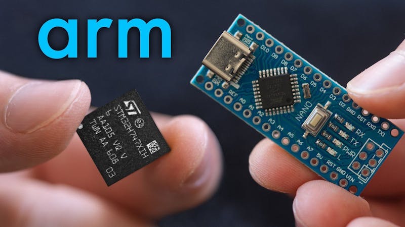
What do you get when you keep the Arduino Nano‘s 45 x 18 mm outline and drop a 300 MHz Arm Cortex-M7 into the spot where the ATmega328P used to sit?
The short answer: a lot more headroom
Maker Magmabow rebuilt the Nano around Microchip’s ATSAME70, a 32-bit Cortex-M7 part. By his own numbers the swap buys roughly 18 times the raw speed, 60 times the program memory, and 200 times the RAM of the 16 MHz AVR on a stock Nano. The pinout still drops into a breadboard, so the mechanical habits you already have carry over while the compute ceiling moves somewhere else entirely. For a thesis group doing sensor fusion or audio DSP that an ATmega328P chokes on, that gap is the difference between “we simplified the algorithm” and “it runs.”
How he escaped the BGA
Routing was the hard part. Dense BGA packages normally need microvias or via-in-pad construction to get traces out from under the chip, and both drag a cheap 2-layer order into expensive territory. Magmabow edited the footprint instead: he deleted pads the design did not need and trimmed the internal ground pads, opening lanes wide enough for ordinary traces to walk out between the survivors. Even after that the board stayed dark. Debugging turned up the real culprit, VDD_OUT has to feed VDD_CORE before the internal core supply will bring the processor up. Bridging the neighbouring capacitor pads with solder woke the chip, and an MPLAB Snap could finally flash firmware.
Power delivery was the second gotcha. A resistor divider reads a tidy 3.3 V on a meter with nothing attached, then sags the instant the core starts switching hard. A linear regulator burns the spare 1.7 V from the USB-C rail as heat, which is unpleasant on a board this small and this thirsty. The shipping revision uses an integrated buck converter to step 5 V down to 3.3 V, with a feedback resistor network setting the output and enough bulk capacitance to ride out sudden current spikes. Magmabow later respun the same layout around an STM32 for comparison.
Try it on your own bench
Do not start at BGA. Lay out a QFP Cortex-M0+ or an STM32G0 on a Nano outline first, get your USB-C buck stage and boot pins correct, then move to ball packages once you know your fab’s minimum trace width and drill specs. A stock Nano and a decent breadboard from circuit.rocks make a fine reference target to measure your clone against. Full build notes and video are on Hackster.
Frequently Asked Questions
Which microcontroller replaces the ATmega328P on this board?
Microchip’s ATSAME70, a 32-bit Arm Cortex-M7 running at 300 MHz. Against the 16 MHz ATmega328P on a stock Nano that works out to roughly 18x the speed, 60x the program memory and 200x the RAM, all inside the same 45 x 18 mm outline.
Why is a BGA package so hard to route on a hobby-budget PCB?
Ball packages put pads under the chip, so traces normally escape through microvias or via-in-pad, both of which cost extra at most fab houses. Magmabow removed unused pads from the footprint and trimmed the internal ground pads, which opened enough space for standard traces on an ordinary board stack-up.
What will I learn if I build this?
You practise fine-pitch footprint editing, escape routing, and switching power supply design: sizing a buck converter, setting a feedback resistor network, and placing decoupling capacitance so the 3.3 V rail survives current spikes. You also get real bring-up debugging experience, the kind where a dead board turns out to be one missing VDD_OUT to VDD_CORE connection.
