
There’s a quiet shift happening in maker hardware: the line between “microcontroller” and “programmable logic” is starting to blur. Boards like the Raspberry Pi Pico taught a generation of students to love Programmable I/O (PIO) for timing-critical tricks, but PIO only stretches so far. When your project needs genuinely custom digital hardware, an FPGA has always been the next step, and that step used to be a steep one. Adiuvo Engineering’s new Forgix board is part of a growing wave of hybrid platforms trying to close that gap.
One board, two very different brains
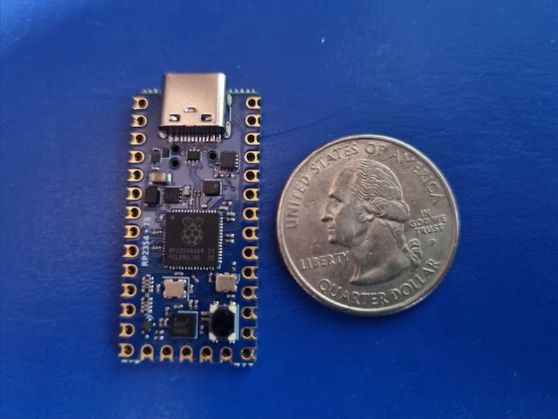
Forgix pairs a Raspberry Pi RP2354 microcontroller with an Efinix Trion T8F49 FPGA that packs 7,384 logic elements. The RP2354’s dual Arm Cortex-M33 cores handle the familiar firmware side of a project, while the FPGA can be reconfigured to build custom peripherals, high-speed signal pipelines, or protocol handlers that would be painful (or impossible) to pull off in software alone. It follows a Teensy-compatible form factor, so it drops straight onto a breadboard, and it breaks out SPI, I2C, UART, USB 1.1, and ADC for talking to sensors and displays.
The technical takeaway
The clever part is how the FPGA gets programmed. Instead of dedicated programming hardware, Adiuvo built an open-source Forge FPGA Loader: a Python GUI or CLI streams an Efinity-generated bitstream over USB serial to the RP2354, which forwards it to the FPGA over SPI. Because the data streams straight through rather than being buffered whole in RAM, the microcontroller’s 520 KB of SRAM never becomes the ceiling on FPGA image size. Add a USB-C connector, an addressable RGB status LED, a user button, and a Tag-Connect SWD header, and you have a debuggable playground for around fifty dollars.
What to try next
If you’ve been curious about FPGAs but scared off by the tooling, a hybrid board like this is a friendly on-ramp. Start by driving an addressable LED strip from the FPGA while the RP2354 runs your app logic, then graduate to a custom SPI peripheral or a small signal-processing block. For an ECE thesis or a robotics-team member who wants to understand what actually happens below the firmware layer, learning to move a task from software into gates is one of the most eye-opening exercises in embedded design.
Frequently Asked Questions
What chips power the Forgix board?
It combines a Raspberry Pi RP2354 microcontroller (dual Arm Cortex-M33 cores, 520 KB SRAM) with an Efinix Trion T8F49 FPGA that has 7,384 logic elements, giving you both firmware and reconfigurable hardware on one board.
How do you program the FPGA without extra hardware?
Adiuvo’s open-source Forge FPGA Loader streams an Efinity-generated bitstream over USB serial to the RP2354, which forwards it to the FPGA over SPI. Because it streams through rather than buffering in RAM, the microcontroller’s memory doesn’t limit the FPGA image size.
What will I learn if I build with this?
You’ll learn to split a design between software and hardware: writing firmware on the Cortex-M33 cores while offloading timing-critical or custom-protocol work into FPGA logic. That includes FPGA bitstream tooling, SPI/I2C/UART interfacing, and the core embedded skill of deciding what belongs in code versus gates.